 ®
®
Transistors and Digital Logic Gates
Southern Polytechnic State University
Copyright © 2000, 2002 by Bob Brown
Flow and Pressure
To begin this Web Lecture, we will take a brief excursion into electrical engineering by way of plumbing!
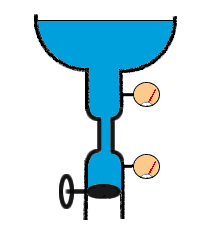
|
| Figure 1. Click to open or close the valve. See what happens to the pressure. |
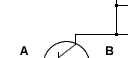
The reservoir is drawn to fit the page; imagine that its capacity is very large -- on the order of that of a municipal water system. In other words, the reservoir will provide water at constant pressure and a high flow rate for a very long time.
When the valve is closed, the pressure is equal on both sides of the constriction. Click on the valve wheel to open or close the valve and observe what happens to the pressure.
When the valve is open, water escapes from the system through the open lower pipe, and the pressure in the lower pipe drops because the rate of supply is limited by the constriction. The pressure above the constriction remains high because of the reservoir supply. In other words, there is a pressure drop across the constricted pipe. The pressure drop occurs only when there is flow through the constriction; when there is no flow, the pressure is constant throughout.
Electrical Pressure
Electricity has "pressure" just as water does. Electrical pressure, or electromotive force, is measured in Volts and is often called voltage. We saw in the previous web lecture that switches could be used to control the flow of electricity. The volume of electrical flow is measured in Amperes and is called current.A switch is an all-or-nothing device like the valve in Figure 1. There are devices that can impede the flow of electricity, similar to the constricted pipe in Figure 1. These are called resistors and they appear as a sawtooth line in a schematic diagram. The relationship among resistance, current and voltage is described by Ohm's Law, which we will not study here.
What is important to students of digital logic is this: If no current is flowing through a resistor, the voltage at the two ends will be the same; if current is made to flow through the resistor, there will be a voltage drop across the resistor. This is analogous to the pressure drop across the constricted pipe of Figure 1. The pressure drops only when water is flowing.
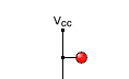
Consider an electric circuit that is conceptually similar to Figure 1.
 |
|||||||
|
|
|||||||
| Figure 2. Click on the switch to change the state of the circuit. | |||||||
In digital logic, it is common to let a "high" voltage, that is a voltage nearly equal to Vcc indicate a logical one, and a "low" voltage -- a voltage near zero -- indicate a logical zero. In the initial state, with the switch open, both LEDs in Figure 2. are on indicating a logical value of one.
Now click on the switch to close it. Closing the switch allows current to flow from Vcc to ground. Because current is flowing, there is a voltage drop across the resistor. The voltage at the lower end, labeled "Output," becomes approximately zero as shown by the extinguished LED. The upper LED remains on because it is connected to Vcc. In future circuits, we will not bother to show the upper LED because it is on all the time.
An important thing to notice about Figure 2. is that the output is true, or one, when the switch is open. This circuit is an inverter; it computes the Boolean NOT function.
Transistors as Switches
At last we are ready to start using transistors! A bipolar junction transistor is an electronic device with three elements called the base, the collector, and the emitter. Transistors can function as analog devices and are used in that way in radios, amplifiers, and similar gear. By choosing suitable transistors and providing suitable inputs, they can also function as digital devices -- switches that are either on or off.Transistors have the property that if a suitable voltage is applied to the base, current can flow between the collector and the emitter. This is exactly like the mechanical switches we've been using except that we control the switching action with voltage instead of mecahnical motion. Switches made in this way can operate at electronic speeds instead of mechanical speeds. The switching speed of a typical transistor is a few nanoseconds -- a few billionths of a second. That's how computers can operate as fast as they do.
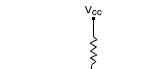
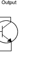
Replacing the mechanical switch with a transistor gives the circuit of Figure 3.
 |
|||||
|
|
 |
||||
| Figure 3. An inverter. Click on the pushbutton to change the voltage at the base of the transistor. | |||||
The pushbutton in the diagram can be used to apply or remove voltage at the base of the transistor. Click on the pushbutton and observe what happens. When voltage is present at the base of the transistor, current flows from collector to emitter, then to ground, and there is a voltage drop across the resistor. The voltage at the output drops to near zero. Removing the voltage at the base stops the current flow and the output voltage rises to be equal to Vcc.
A transistor used in this way is an amplifier as well as a switch. A voltage lower than Vcc is enough to make the transistor switch on; very little current flows from the base to ground through the emitter. A much larger current flows from collector to emitter and then to ground. The transistor is a current amplifier, but the important part of the circuit is the voltage change at the output, from near Vcc when the transistor is switched off to near zero when the transistor is switched on.
Like the circuit in Figure 2, this circuit is an inverter. The output is high when the input is low and vice-versa. This circuit computes the Boolean NOT function. (If you are troubled by the lack of a second connection on the pushbutton and the LED, refer to the section on abstraction in the previous Web Lecture.)
NAND and NOR Gates
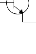
 |
|||||
|
|
 |
||||
|
|
|||||
| Figure 4. A NAND gate. The value of the output is controlled by the two inputs A and B. | |||||
For purposes of this lecture we are going to define a "high" voltage -- a voltage near Vcc -- to indicate a logical 1, or true. A low voltage, near zero will indicate a logical 0, or false. (It is possible to reverse those definitions so long as one is consistent. We will not study negative logic circuits here.)
| A | B | X | |||
|---|---|---|---|---|---|
| 0 | 0 | 1 | |||
| 0 | 1 | 1 | |||
| 1 | 0 | 1 | |||
| 1 | 1 | 0 |
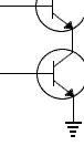
It is clear from the schematic diagram that we could build a NAND gate with more than two inputs. Adding a third transistor in series gives a three-input NAND. As an exercise, write the truth table for a three-input NAND gate. You will have inputs A, B, and C and output X.
 |
|||||||
 |
 |
||||||
|
|
 |
|
|||||
| Figure 5. A NOR gate. The transistors are connected in parallel. | |||||||
The NAND gate has its transistors connected in series. Recall from the Electric Circuits Web Lecture that switches can be connected in series or parallel. If we connect transistors in parallel as shown in Figure 5, applying a signal to the base of either transistor is sufficient to allow current to flow through the resistor and pull the output voltage to near zero. This is the NOR gate. The name NOR is a contraction of not-or.
| A | B | X | |||
|---|---|---|---|---|---|
| 0 | 0 | 1 | |||
| 0 | 1 | 0 | |||
| 1 | 0 | 0 | |||
| 1 | 1 | 0 |
Let's look at the truth table for the NOR gate. Again we have inputs A and B and output X. This time, X is true, or 1, only when A and B are both 0. Another way of saying that is that X is 1 when neither A nor B is true. Experiment with the circuit to verify that it computes the function given in Table 2.
As with the NAND gate, the NOR gate can be extended to more than two inputs by adding more transistors, this time in parallel.
Figure 5 makes it obvious why the power supply voltage is called Vcc. It is connected in parallel, or in common, through the resistor to the collectors of both transistors. In a complex digital logic circuit, the same power supply voltage will be connected in common to all the gates.
About now you may be wondering why we started with NAND and NOR gates instead of the more familiar AND and OR functions. There are two reasons, one founded in electrical engineering and one founded in logic.
Although the gates shown here are simplified by comparison to the actual construction of integrated circuits, you could go to an electrical engineering lab and build the circuits of Figures 3, 4, and 5. If you did, they would function just as the animations demonstrate. These three gates, NOT, NAND, and NOR are the simplest possible digital logic gates. Each has only one transistor per input. Any other gate, and in particular the non-inverting gates AND and OR require more transistors.
Even more important is the fact that NAND and NOR are complete. This means that any other digital logic gate can be constructed using only NAND gates or only NOR gates. A manufacturer of integrated circuits can lay down a pattern of one type of gate, and then implement any digital logic function by modifying how the gates are connected.
Digital Logic Symbols
We generally don't draw individual transistors in diagramming digital logic circuits. Instead we use abstraction to suppress unnecessary detail and represent only the required information. We need to show three things about each digital logic gate: the function of the gate, the inputs, and the output. The internal construction of the gate and certain connections are suppressed.
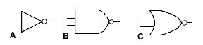 |
| Figure 6. Digital Logic Symbols. A. NOT, B. NAND and C. NOR gates. |
The bullet shape is an AND gate; adding the circle makes it a NAND gate.
The shield shape is an OR gate; with a circle it becomes a NOR gate.
The inputs are shown as wires at the left of each gate, and the output is a wire on the right. Real gates require connections to Vcc and ground in addition to their inputs and outputs. These connections are not shown on digital logic symbols, but are assumed to be present. This is another example of abstraction.
The circle at the output end of each gate is called an inversion bubble. It indicates that the output is inverted. Table 1 is the truth table for a NAND gate; each bit of the output is the complement, or inverse of the corresponding bit for the AND function. Similarly, the truth table for NOR shown in Table 2 is the inverse of the OR function.
We have examined the way three types of digital logic gates are constructed. In the next Web Lecture we will derive some other types of gates and build a simple digital logic circuit.
Click here to provide comments and feedback on this Web Lecture.
Table of Contents![]() Previous: Electric
Circuits
Previous: Electric
Circuits![]() Next: More Digital Logic Gates
Next: More Digital Logic Gates
There are other kinds of transistors than the bipolar junction transistor, more commonly used in making chips. The BJT works well as an example, and we will use it that way.
Copyright © by Bob Brown. Some rights reserved.
This work is licensed under a Creative Commons Attribution-NonCommercial-ShareAlike 3.0 Unported License.
Last updated:
2016-06-11 12:58
Originally published:
2000-08-26