Introduction to Sequential Circuits
Southern Polytechnic State University
Copyright © 2000 by Bob Brown
Sequential Circuits
We said that the output of a combinational circuit depends solely upon the input. The implication is that combinational circuits have no memory. In order to build sophisticated digital logic circuits, including computers, we need more a powerful model. We need circuits whose output depends upon both the input of the circuit and its previous state. In other words, we need circuits that have memory.
For a device to serve as a memory, it must have three characteristics:
- the device must have two stable states
- there must be a way to read the state of the device
- there must be a way to set the state at least once.
It is possible to produce circuits with memory using the digital logic gates we've already seen. To do that, we need to introduce the concept of feedback. So far, the logical flow in the circuits we've studied has been from input to output. Such a circuit is called acyclic. Now we will introduce a circuit in which the output is fed back to the input, giving the circuit memory. (There are other memory technologies that store electric charges or magnetic fields; these do not depend on feedback.)
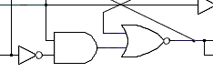
The S-R Latch
The output of a NOR gate is true only when both inputs are false. Consider the circuit in Figure 1. The output of each NOR gate is fed back to the input of the other.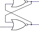 |
|||||||
| Figure 1.
The S-R Latch. S sets the latch, causing Q to become true. R
resets the latch. | |||||||
For the output of the upper NOR to be true, both its inputs have to be false. Examine the circuit and you will see that this is also correct.
Now press the S
button. The output of the upper NOR gate, ![]() is forced to false, allowing the
output of the lower NOR to become true.
is forced to false, allowing the
output of the lower NOR to become true.
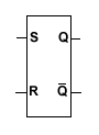
Figure 1-B. The symbol for the S-R latch.
With S off, turn R on, then off again. What happens? Why.
This circuit is an S-R latch. An S-R latch is also called a
set-reset latch. An input on S sets the latch, making
![]() true and
true and
![]() false.
An input on
R resets the
latch;
false.
An input on
R resets the
latch;
![]() becomes false and
becomes false and
![]() becomes true.
The output of the circuit is stable in either state with the inputs
removed. We can remove the input that caused a particular output and the
output will be unchanged.
The state, and so the output, will only change when the complementary input
is applied. Such a circuit is said to be bistable because it has two
stable states.
becomes true.
The output of the circuit is stable in either state with the inputs
removed. We can remove the input that caused a particular output and the
output will be unchanged.
The state, and so the output, will only change when the complementary input
is applied. Such a circuit is said to be bistable because it has two
stable states.
The symbol for the S-R latch is shown in Figure 1-B. Whether the
![]() output is
available depends upon how the latch is packaged and whether an extra
pin is available.
output is
available depends upon how the latch is packaged and whether an extra
pin is available.
The input S=R=1 is not allowed. If both inputs are true, both outputs
must be false. This implies ![]() =
=![]() =0,
which is logically inconsistent. Further, the circuit is unstable in this
state; when one of the inputs returns
to the false state, the remaining input determines the stable state and
the output changes.
=0,
which is logically inconsistent. Further, the circuit is unstable in this
state; when one of the inputs returns
to the false state, the remaining input determines the stable state and
the output changes.
We use the word latch here to mean a circuit that can store one bit. A register that supplies data to the inputs of a combinational circuit is also called a latch; we will encounter this second meaning of the word later.
Note: The circuits above have been drawn with S and ![]() at the top to be consistent with
Tanenbaum. Most other textbooks place R and
at the top to be consistent with
Tanenbaum. Most other textbooks place R and ![]() at the top. Since the circuit
is symmetrical, exchanging the labels makes no difference so long as both
the input and output labels are exchanged.
at the top. Since the circuit
is symmetrical, exchanging the labels makes no difference so long as both
the input and output labels are exchanged.
Timing Considerations
Before we go further, we need to consider what happens when the outputs of two or more gates are combined to form the output of a combinational circuit. We have discussed the fact that the switching time of a transistor is a few nanoseconds, but we haven't emphasized the fact that this switching time causes a finite time delay between a change in the inputs of a gate and any change in the output. This time is called gate delay. So far, we have ignored gate delay, and so do simple circuit simulators.Figure 2 shows a combinational circuit adapted from [MURD00]; in ordinary circumstances, the three inputs A, B, and C would come from other circuits. We've wired them all to one pushbutton to make a point. If you study the circuit, you will see that the output should be zero or false regardless of the input. If the input is zero, both A and BC will be zero and the XOR gate will produce a zero. If the input is a one, A and BC will be ones, and the
| Figure 2. This circuit can produce a glitch. | |||||||||
With all inputs off, the AND gate produces an output of false, both inputs to the XOR gate are false, and the output of the circuit is false. Press the pushbutton and observe carefully what happens. (Cycle from off to on and back a few times if you need to.) The A input to the XOR gate becomes true, and the BC inputs to the AND gate also become true. However, the output of the AND gate remains false for a time equal to one gate delay. The XOR gate has inputs of true-false, and will produce an output of true one gate delay later.
After one gate delay has passed, the output of the AND gate is true and the input of the XOR gate is true-true. However, the output of the XOR gate remains true for one gate delay time. After the second gate delay time, the output of the XOR gate attains the correct value of false. The process reverses itself when the pushbutton is turned off. Experiment with the circuit until you are sure you understand what is happening.
A circumstance where timing dependencies can briefly cause incorrect output is called a hazard. Now consider what would happen if the output of Figure 2 were connected to the S input of an S-R latch. The latch could be set to true when it should not be. Storing an incorrect value in this way is called a glitch.
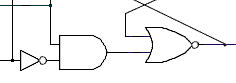
Clocking
In order to avoid glitches, we want to design storage elements that only accept input when ordered to so. We will give the order only after the combinational circuits that compute the input to the storage device have had a chance to settle to their correct values.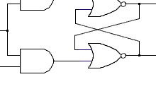 |
|||||||
| Figure 4.
A clocked S-R latch. The latch can change only when C is
true. |
|||||||
When the control signal is true, the S and R signals are propagated through the AND gates and the stored value can change.
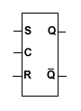
Figure 4-B. The symbol for the clocked S-R latch.
The circuit of Figure 4 is a clocked S-R latch. With the C
input false, experiment with the S and R inputs. Now make the C
input true by pressing the button and experiment again with S and R.
Note that clocking does not help with the problem of S=R=1. In fact,
it makes the problem worse. With S and R both true, turn C on and off
several times. You cannot predict whether the latch will store
![]() or
or
![]() . When the S
and R inputs are removed simultaneously, the latch settles into one of
its two stable states at random.
. When the S
and R inputs are removed simultaneously, the latch settles into one of
its two stable states at random.
The Clocked D-Latch
Once we have applied the idea of clocking to our S-R latch, we can get rid of the problem of what to do with S=R=1 and also simplify the input to our circuit.Usually what we want to do with a storage device is store one bit of information. The need for explicitly setting and resetting the latch is added complexity.
 |
|||||||
| Figure 5. A clocked D-latch. When C (control) is true, the value at D (data) is stored in Q. | |||||||
The circuit of Figure 5 is such a circuit. It has a data input, D, and a control input, C. The data input is connected through an AND gate to the S input of an S-R latch. It is also connected through an inverter and an AND gate to the R input. The other inputs of the two AND gates are connected to the C input of the circuit. If C is false, no signals reach the latch and its state remains unchanged. If C is true and D is true, the S input of the latch is true and the latch stores a value of true, which is equal to D. If C is true and D is false, the R input of the latch is driven through the inverter and a value of false, which is equal to D, is stored. Experiment with the circuit and observe what happens.
Here is something to think about: The concept of a D latch, where
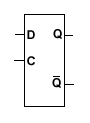
Figure 5-B. The symbol for the clocked D latch.
The clocked D-latch stores whatever is on the D input when C is true. If C is asserted (made true) only after the input circuits have settled, this circuit will store the correct value of D. Because there is only one data input, the case of S=R=1 cannot occur.
Make C true by operating the pushbutton, then change the value of D
and watch what happens. As long as the C input is true, changes to
D are reflected in the output of the circuit. The clocked D-latch is
a level triggered device. Whether it stores data depends upon
level at C.
Master-Slave Flip-Flops
The clocked D-latch solves several of the problems of storing output from a combinational circuit, but not all of them. Particularly, if D changes while C is true, the new value of D will appear at the output. Generally this is not what is wanted. If the stored value can change state more than once during a single clock pulse, the result is a hazard that might introduce a glitch later in the circuit. We must design the circuit so that the state can change only once per clock cycle. This can be accomplished by connecting two latches together as shown in Figure 6. The left half of the circuit is the clocked D-latch from the previous section. The right half of the circuit is a clocked S-R latch; however, the clock signal for the output section is the input clock signal inverted. The output of this device can only change once per clock cycle. The change occurs shortly after the falling edge of the clock cycle.Here's why: Starting with the clock low, the left half of the circuit cannot change state because the inputs are inhibited by the low clock. The AND gates prevent the inputs from reaching the latch. The right half of the circuit could change because it "sees" a high clock, but its inputs come from the latch on the left, and they can't change.
When the clock signal goes high, the D input can change the state of the left latch. One gate delay later, the clock input of the right latch goes low. Since there are at least two gate delays through the D latch that is the left half of the circuit, the right latch cannot change state before its clock signal goes low. With the clock signal high, D can change, and the left latch will change also. However, the output will not change.
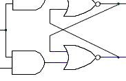 |
|||||||||
 |
|||||||||
| Figure 6.
A Master-Slave D Flip-Flop.
The output of this device does not change until the clock signal goes
low. |
|||||||||
The output of a master-slave flip-flop can change only at the falling (or rising, if designed that way) edge of the clock pulse. That's why we call it a flip-flop instead of a latch.
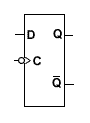
Figure 6-B. The symbol for the D flip-flop.
The symbol for the D flop-flop is shown in Figure 6-B. The triangle at
the clock input indicates that this device changes state only on clock
transitions. The negation bubble indicates that the change is on the
"negative" or falling edge of the clock.
The master-slave flip-flop is an adequate design for a D flip-flop. There
are other types of flip-flops, not studied here, for which it doesn't
work. The J-K flop-flop, for example, exhibits a phenomenon known as
ones-catching in the master-slave configuration. A spurious one on the
input will be latched and propagated to the output even if the input
returns to zero before the end of the clock period.
Edge Triggered Devices
We could solve the problems of hazards and ones-catching if we could design a memory that would both sample its inputs and store data based on the transition of a clock pulse. If the combinational parts of a circuit could settle during the time the clock signal was true, and the storage part of the circuit sampled the input and saved the result when the clock changed from true to false, we would have no problems with hazards at the output nor with ones catching. A storage circuit like that is called a negative edge-triggered flip-flop. A circuit that stores a result on transition of the clock from false to true is a positive edge-triggered flip-flop.
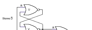 |
|||||||
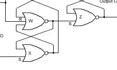 |
|||||||
| Figure 7. This circuit is triggered by the falling edge of the clock. | |||||||
Here is how it works: When the clock is true, the S input of latch U-V and the R input of latch W-X are also true. This forces the S and R inputs of latch Y-Z to false, and the circuit cannot change state. When the clock changes from true to false, D appears on the S input of latch Y-Z and the complement of D appears on the R input. Output Q reflects the value of D.
When the clock is false, one of the inputs to Y-Z is true and the other is false. Latches U-V and W-X are stable in this state regardless of changes in D. Latch Y-Z, and therefore the output of the circuit, can only change on the true-to-false clock transition.
Let's examine the assertion that the latches U-V and W-X are stable when the clock is low. At the falling edge of the clock, either Y's R must be true or Z's S, but not both. Consider the case that Y's R is true. This means V's inputs must both be false. That the clock is false is given. V's other input comes from U; U's lower input comes from V and is true from the assumption that Y's R is true. Therefore, U's output must be zero and the output of latch U-V is stable regardless of changes in D.
The alternative assumption is that Z's S is true, meaning that the ouptut of W is true. All three of W's inputs must be false. Clock is false by assumption.The upper input of W is false given the assumption that the output of V is false. If the output of W is true, the upper input of X is true, the output of X is false, and the lower input of W is false. The output of W is stable when the clock is low regardless of changes in D.
By experimenting with the circuit, verify that changing D has no effect
on the output regardless of whether the clock is high or low. The
output changes to reflect the current state of D only when the clock
changes from high to low.
Please take a moment to
Web Lectures Table of Contents
References
[MURD00] Murdocca, Miles J. and Vincent P. Heuring, Principles of Computer Architecture, Prentice-Hall, 2000.[TANE99] Tanenbaum, Andrew S., Structured Computer Organization, Prentice-Hall, 1999.
Copyright © 2000 by Bob Brown. Some rights reserved.
This work is licensed under a Creative Commons Attribution-NonCommercial-ShareAlike 3.0 Unported License.
Last updated: 2012-10-21 21:59
Orignially published: 2000-10-01